CL_AXIL_REG_ACCESS#
Table of Contents#
Overview#
The goal of cl_axil_reg_access is to demonstrate: 1. Writing two 32-bit registers on the FPGA, performing an addition operation, and reading the result back to the host using the OCL interface 2. Attaching Integrated Logic Analyzer (ILA) and Virtual JTAG to monitor AXI-Lite traffic
Block Diagram#
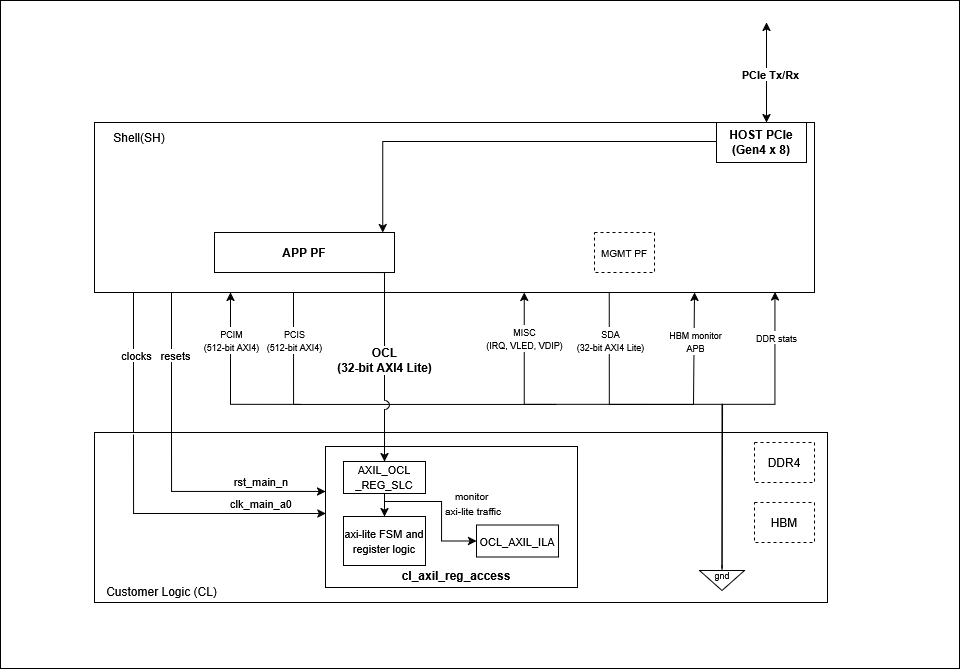
Block Diagram of cl_axil_reg_access#
Functional Description#
OCL AXI-Lite Interface#
OCL is a 32-bit wide AXI-Lite
interface
that provides a communication channel between the host and FPGA. It has
a 32MiB register space available (from 0x00000000 to 0x01FFFFFF)
in the custom logic (CL) for register access, control, and monitoring
operations. This address space is associated with PCIe Application PF0
and BAR0. Read more about PCIe BARs
here.
The register map for this example is defined as follows:
OCL Address |
Register name |
Access |
Register Description |
|---|---|---|---|
0x0000_0000 |
Operand_A |
RW |
Bit [31:0]: Holds an unsigned 32-bit integer |
0x0000_0004 |
Operand_B |
RW |
Bit [31:0]: Holds an unsigned 32-bit integer |
0x0000_0008 |
Sum |
RO |
Bit [31:0]: Holds an unsigned 32-bit integer |
0x0000_000C |
Carry |
RO |
Bits [31:1]: Reserved, assigned to 0<br>Bit [0]: Carry output from addition |
0x0000_0010 |
Control_Status |
RW |
Bits [31:2]: Reserved, assigned to 0<br>Bit [1]: Ready bit (RO, indicates result is ready)<br>Bit [0]: Start bit (write 1 to trigger operation) |
Note: - RW (Read-Write): Register can be both read from and
written to by the host - RO (Read-Only): Register can only be read
by the host - Any access to addresses outside this range will return
0xDEADBEEF
Configuration Sequence#
For software runtime, follow this configuration sequence:
Write operands — write input values to
Operand_AandOperand_BregistersTrigger addition — write
1to bit [0] ofControl_Statusregister; this starts the addition and computes{Carry[0], Sum} = Operand_A + Operand_BPoll for completion — read bit [1] of
Control_Statusregister and wait until it is set to1; this indicates the result is readyRead results — read
SumandCarryregisters; bit[1] ofControl_Statusregister is automatically cleared after these registers have been read
Functional Code Blocks#
Register Access#
Register Write:
Write operations update registers in the WRITE state, when both
address and data handshakes are complete:
// Register writes
always_ff @(posedge clk_main_a0) begin
  if (next_state == WRITE) begin
    case (write_addr)
      ADDR_OPERAND_A : reg_operand_a <= sh_ocl_wdata_q;
      ADDR_OPERAND_B : reg_operand_b <= sh_ocl_wdata_q;
    endcase
  end
end
Register Read:
Read operations return register values when the read address handshake
completes. Invalid addresses return 0xDEADBEEF:
// Register reads
always_ff @(posedge clk_main_a0) begin
  if (addr_rd_handshake) begin
    case (sh_ocl_araddr_q)
      ADDR_OPERAND_A       : ocl_sh_rdata_q <= reg_operand_a;
      ADDR_OPERAND_B       : ocl_sh_rdata_q <= reg_operand_b;
      ADDR_SUM             : ocl_sh_rdata_q <= reg_sum;
      ADDR_CARRY           : ocl_sh_rdata_q <= reg_carry;
      ADDR_CONTROL_STATUS  : ocl_sh_rdata_q <= reg_control_status;
      default              : ocl_sh_rdata_q <= INVALID_ADDR_RESP;
    endcase
  end
end
AXI-Lite FSM#
The AXI-Lite interface is controlled by a 5-state FSM:
State |
Description |
|---|---|
|
Ready to accept a new transaction. awready and wready asserted for write; arready asserted for read |
|
One write channel (address or data) arrived first — waits for the other |
|
Both address and data are valid; register write executes this cycle |
|
Sends write response (bvalid); waits for bready from the host |
|
Read data presented on rdata (rvalid asserted) |
always_comb begin
  next_state = current_state;
  case (current_state)

    IDLE: begin
      if (addr_wr_handshake && data_wr_handshake)
        next_state = WRITE;
      else if (addr_wr_handshake || data_wr_handshake)
        next_state = WRITE_WAIT;
      else if (addr_rd_handshake)
        next_state = READ;
    end

    WRITE_WAIT: begin
      if (addr_wr_handshake || data_wr_handshake)
        next_state = WRITE;
    end

    WRITE: begin
      next_state = WRITE_RESP;
    end

    WRITE_RESP: begin
      if (bresp_handshake)
        next_state = IDLE;
    end

    READ: begin
      if (data_rd_handshake)
        next_state = IDLE;
    end

    default: begin
      next_state = IDLE;
    end
  endcase
end
Virtual JTAG#
One ILA core is attached to the OCL AXI-Lite bus. Virtual JTAG access is enabled via MgmtPF BAR2 using the debug bridge. Refer to the Virtual JTAG Debug Guide to connect Vivado Hardware Manager to the XVC server for real-time register monitoring and debugging.
Clock and Reset#
This example uses clk_main_a0 clock at 250MHz and rst_main_n
reset provided by the AWS Shell to the CL.
Resource Utilization#
Resource |
Used |
Utilization |
|---|---|---|
CLB LUTs |
3,412 |
0.26% |
CLB Registers |
335 |
<0.01% |
CLB |
1,634 |
1.00% |
URAM |
0 |
0.00% |
DSPs |
0 |
0.00% |
CARRY8 |
5 |
<0.01% |
RTL Simulation#
For detailed descriptions of all simulation tests and how to run them, refer to verif/README.md.
Software Runtime#
The runtime examples are located in the software/runtime directory.
To compile and run a test:
cd $CL_DIR/software/runtime
make all
sudo ./test_sum
This example includes software tests demonstrating register-based
communication via the OCL interface. All tests use utility functions
from cl_axil_reg_access_utils.c.
FPGA API Functions#
fpga_pci_attach() establishes a connection to a specific PCIe BAR on
the FPGA. It takes the slot ID, physical function (PF) ID, BAR ID,
flags, and returns a handle for accessing that BAR’s memory space. This
is done before performing any register access:
// Attach to OCL BAR
rc = fpga_pci_attach(slot_id, pf_id, bar_id, flags, &pci_bar_handle);
Writing to OCL registers:
// Write operand A at address 0x0000
fpga_pci_poke(pci_bar_handle, 0x0000, operand_a);

// Write operand B at address 0x0004
fpga_pci_poke(pci_bar_handle, 0x0004, operand_b);
Reading from OCL registers:
// Read sum result at address 0x0008
fpga_pci_peek(pci_bar_handle, 0x0008, &result);
📓 For an interactive, step-by-step walkthrough of the software runtime example, refer to the cl_axil_reg_access Jupyter notebook.