HLx Flow for Hello World IP Integrator Example#
Table of Contents#
Overview#
This IP Integrator design includes the AWS IP configured with an OCL interface (AXI4-Lite Master) that controls the VLED through AXI GPIO and a PCIS interface (AXI4 Master) that performs read and write operations to the AXI BRAM in the CL.
The VLED is set based upon writing 0xAAAA into the AXI GPIO (0x0)
slave register to drive the VLED. The value is read using the Verilog
task tb.get_virtual_led in simulation or fpga-get-virtual-led on
F2 instance.
The PCIS Interface writes ASCII data into the AXI BRAM memory space and reads back from these addresses to print out “Hello World!” in simulation or on a F2 instance.
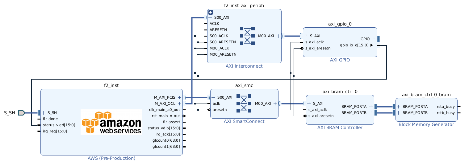
block-diagram#
Building and Testing Example#
Follow the common design steps specified in the IPI example design flow document to build and test this example on F2 instances.