CL_DRAM_HBM_DMA CustomLogic Example
⚠️ Features using XDMA engine are currently unsupported on F2 instances
Table of Content
Overview
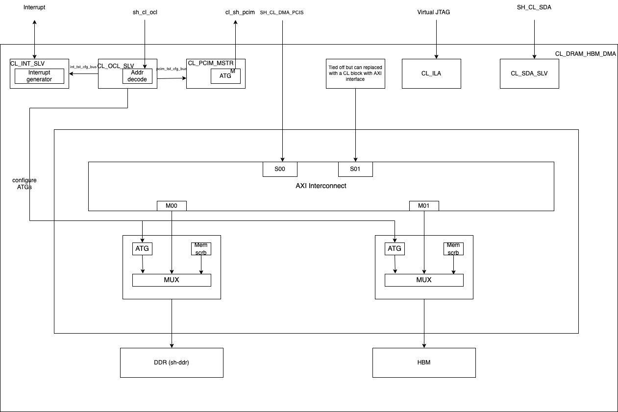
The CL_DRAM_HBM_DMA example demonstrates the use and connectivity for many of the Shell/CL interfaces and functionality, including:
Register access over OCL AXI-Lite interface
Mapping of the external DRAM channel to instance memory via PCIe AppPF BAR4, and the 512-bit
sh_cl_dma_pcis_*AXI4 busMapping of HBM memory to instance memory via PCIe AppPF BAR4, and the 512-bit
sh_cl_dma_pcis_*AXI4 busDebugging using Virtual JTAG and Xilinx Integrated Logic Analyzer (ILA) cores.
User-defined interrupts
cl_sh_pcim_*AXI4 traffic for Host memory accesses from CL
System diagram
Functional Description
Memory Interface
The cl_dram_hbm_dma demonstrates accessing 64GB of DDR memory and 16GB
of single channel HBM memory over the sh_cl_dma_pcis AXI4 bus.
The CL provides access to the DDR memory through sh_ddr.sv which
consists of the DDR controller required to interact with the external
DDR DIMM on the FPGA card. The sh_ddr.sv is also connected to the
Shell’s sh_cl_ddr_stat_* ports to enable Shell to manage DDR
calibration upon CL AFI loads.
The CL also provides access to the on-chip HBM available in the FPGA.
The HBM IP is configured for dual stack 16GB capacity which exposes 32
AXI3 (not AXI4) channels running on 450MHz clock. However, only one HBM
channel is being used in this example design to demonstrate datapath
connection to the HBM. The cl_hbm_axi4.sv
does the AXI4-to-AXI3 conversion, crosses clock domain between
the 250 MHz clk_main_a0 and HBM’s up to 450 MHz axi_clk for the datapath and feeds
the cl_hbm_wrapper.sv. The
cl_hbm_wrapper.sv instantiates the HBM
IP, houses MMCM to generate 450MHz interface clock, and connects the
datapath to Channel#0 of the HBM IP core.
NOTE: Since the CL utilizes only one HBM Channel which is fed by data source running at 250MHz clock, it does not accomplish the max available bandwidth from HBM. For demonstration of the max performance from HBM. refer to the cl_mem_perf example.
Design Changes
Individual controllers (DDR, HBM) can be enabled and disabled by simply updating the appropriate defines in the cl_dram_hbm_dma_defines.vh file. The sh_ddr.sv file contains the necessary logic to remove and tie-off appropriate interfaces when the DDR controller is disabled.
For the cl_dram_hbm_dma example memory ranges have been allocated for DDR and HBM. So, if a particular memory is disabled, then the developer should take care to handle transactions to that address range since there will be no controller to respond to the request. The address ranges for each controller is described below in the dma_pcis AXI4 bus section.
Test Changes
If a particular controller is disabled, make sure that the test is not accessing address space for that controller.
Please look at dma_pcis AXI4 bus section for address ranges.
If DDR is enabled, make sure that the DDRs are initialized using the poke_stat commands below.
eg: To initialize DDR
tb.poke_stat(.addr(8'h0c), .ddr_idx(0), .data(32'h0000_0000));
Make sure that the Host to Card and Card to Host DMA transfers only access enabled DDR controller address space.
dma_pcis AXI4 bus
sh_cl_dma_pcis exposes a address windows of 128GB matching AppPF BAR4.
This memory space is mapped to the 64GB DRAM space and 16GB HBM space. An axi_crossbar interconnects the incoming address requests to the target memories as shown below:
DDR base_addr=0x00_0000_0000 (range=64GB)
HBM base_addr=0x10_0000_0000 (range=16GB)
NOTE: Please refer to
Supported DDR Modes for
details on supported DDR configurations in sh_ddr.sv.
ocl_ AXI-Lite
The cl_ocl_ AXI-Lite bus is connected to cl_ocl_slv.sv module, and is used for register access to the Automatic Test Generator (ATG) etc.
The valid address map is as shown below:
Module |
OCL Start Address |
OCL End Address |
Description |
|---|---|---|---|
PCIM ATG |
0x0000 |
0x00FF |
PCIM Traffic Generator (refer to |
DDR ATG |
0x0100 |
0x01FF |
DDR Traffic Generator |
HBM ATG |
0x0200 |
0x02FF |
HBM Traffic Generator |
HBM Status |
0x0300 |
0x0300 |
|
Any access to invalid address shall return 32'hDEADBEEF
sda_ AXI-Lite
The sh_cl_sda_ AXI-Lite bus is connected to cl_sda_slv.sv module, which provides 1KiB of scratch RAM.
Address bits [9:0] will be used to access the location of the RAM, but the upper bits of the address are ignored.
pcim_ AXI4
The cl_sh_pcim_ AXI4 bus is driven by Automatic Test Generator (ATG) and connected to cl_pcim_mstr.sv. It can be used to read/write from the host memory.
irq/ack
cl_int_slv.sv provides an example for generating the IRQ requests and checks if ACK has been received.
Virtual JTAG
3 ILA cores are integrated, one to monitoring the sh_c_dma_pcis bus, one to monitor the AXI4 signals on DDR and the third to monitor the AXI4 signals on HBM. An example usage is provided in cl_ila.sv. An example usage for Xilinx VIO is provided in cl_vio.sv
Clocks
CL_DRAM_HBM_DMA uses the main clk_main_a0. It’s frequency is set in
cl_timing_user.xdc
Software
DMA accesses rely on the XDMA driver
The DRAM_HBM DMA example includes runtime software to demonstrate working DMA accesses. The runtime example is located in the runtime directory
There are three example tests in cl_dram_hbm_dma example.
test_dram_dma.c
This test runs a software test with data transfer with DDR enabled.
test_hbm_dma.c
This test runs a software test with data transfer with HBM enabled.
test_dram_hbm_dma.c
This test runs a software test with data transfer with both DDR and HBM enabled
Compile and run instructions
cd ${CL_DIR}/software/runtime
make all
sudo ./test_dram_hbm_dma
test_dram_hbm_dma_hwsw_cosim.c
This test runs a software test with HW/SW co-simulation enabled with both DDR and HBM enabled.
Compile and run instructions
cd ${CL_DIR}/software/runtime
make TEST=test_dram_hbm_dma_hwsw_cosim
sudo ./test_dram_hbm_dma_hwsw_cosim
The test can be simulated with XSIM as follows.
cd ${CL_DIR}/verif/scripts
make C_TEST=test_dram_hbm_dma_hwsw_cosim